Piezoceramic compacts are manufactured from spray-dried granular material by mechanical hydraulic pressing. The compacts come in different shapes as disks, plates, rods, and cylinders. They are either manufactured true to size, taking into account the sintering contraction, or with machining allowances which are then reworked to achieve the required precision.
A large selection of press molds in different geometries and sizes are available. Compacts can be manufactured with dimensions of up to 80 mm in diameter and 50 mm in height. The compact can be reworked by milling, as long as it is still in the green state, i.e., prior to sintering.
The Sintering takes place at temperatures of up to approx. 1300°C. This leads to a shrinkage of the body volume by approx. 15%. The result is a solid ceramic of high density.

The sintered ceramic is hard and can be sawn and machined, if required. Components such as disks or plates can be manufactured at low cost with a minimum thickness from as low as 0.2 mm.
Inboard automatic cutoff saws produce such pieces in large numbers. Modern CNC technology allows for the sintered ceramic elements to be machined with highest precision. Holes with diameters of as low as 0.3 mm can be produced.
Almost any contours can be shaped with accuracies to one tenth of a millimeter. Surfaces can be structured and the components can be milled three-dimensionally for optimum fit.
Ultrasonic machining processes are used to manufacture thin-walled tubes with wall thicknesses of 0.5 mm.


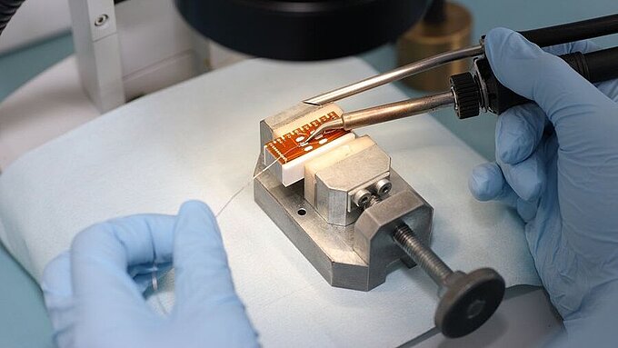
Metallization of the Piezo Elements: Application of the Conducting Electrodes
Thick-film electrodes are applied to the piezo ceramic by screen printing technology. Typical film thicknesses are around 10 µm. Various silver pastes are used in this process. After screen printing, these pastes are baked at temperatures above 800°C.


Thin-film electrodes are applied to the ceramic using modern PVD processes (sputtering). The typical thickness of the metallization is in the range of 1 µm. Shear elements must be metallized in the polarized state and are generally equipped with thin-film electrodes. In high-throughput sputtering facilities, the conducting layers made of metal alloys; preferably CuNi alloys and noble metals, such as gold and silver, are applied.


Polarization

Following the production process, the components are polarized at field strengths up to 3000 V/mm. After >> Polarization, whenever an electric field is applied that is less strong than the original polarization field strength, the ceramic expands.
The finished sintered, machined, polarized, and tested plates or disks can be glued together as stack actuator modules: >> Assembling Technology